Michigan State University combined terahertz laser light, represented by a red wavy arrow, with the tip of a scanning tunneling microscope (STM) — the dark pyramid shape exchanging a red electron with a sample represented by a blue surface. Credit: Eve Ammerman
One of the challenges of integrating smarter, more powerful electronics into ever-smaller devices is developing the tools and techniques to analyze the materials they are made of with ever-increasing precision.
Physicists at Michigan State University have taken a long-awaited step forward in this field with an approach that combines high-resolution microscopy with ultrafast lasers.
The technique, described in the journal Photonics of natureallows researchers to spot mismatched atoms in semiconductors with unprecedented precision. Semiconductor physics calls these atoms “defects,” which sounds negative, but they are usually added to materials intentionally and are critical to the performance of semiconductors in today’s and tomorrow’s devices.
“This is particularly relevant for components with nanoscale structures,” said Tyler Cocker, Jerry Cowen Professor of Experimental Physics and leader of the new study.
This includes things like computer chips, which commonly use semiconductors with nanoscale features. Researchers are working to push nanoscale architecture to the extreme by designing materials that are just one atom thick.
“These nanoscopic materials are the future of semiconductors,” said Cocker, who also directs the Ultrafast Terahertz Nanoscopy Lab in MSU’s Department of Physics and Astronomy. “When you have electronics at the nanoscale, it’s really important to make sure that the electrons can move the way you want them to.”
Defects play an important role in the movement of electrons, so scientists like Cocker want to know precisely where they are and how they behave. Cocker’s colleagues were excited to learn that his team’s new technique will allow them to easily obtain this information.
“One of my colleagues said to me, ‘I hope you guys came out to celebrate,’” Cocker said.
Vedran Jelic, a postdoctoral researcher in Cocker’s group who now works at the National Research Council of Canada, is the first author of the new report. The research team also included doctoral students Stefanie Adams, Eve Ammerman and Mohamed Hassan, as well as undergraduate researcher Kaedon Cleland-Host.
Cocker added that the technique is simple to implement with the right equipment, and his team is already applying it to atomically thin materials like graphene nanoribbons.
“We have a number of projects going on where we’re using this technique with more, more exotic materials,” Cocker said. “We’re integrating it into everything we do and using it as a standard technique.”

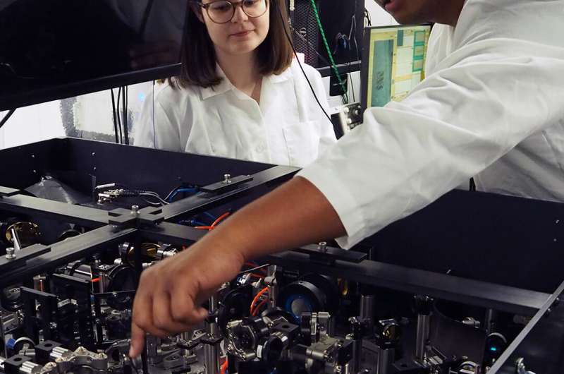
PhD students Mohamed Hassan and Stefanie Adams inspect an optical table to adjust the laser light used in the Michigan State University team’s new technique. Credit: Matt Davenport/MSU College of Natural Science
A light touch (almost)
There are already tools, including scanning tunneling microscopes, or STMs, that can help scientists spot defects in a single atom.
Unlike the microscopes many are familiar with in high school science class, STMs don’t use lenses or light bulbs to magnify objects. Instead, STMs scan the surface of a sample using an atomically sharp tip, much like the stylus on a record player.
But the STM tip doesn’t touch the sample surface, it just gets close enough that electrons can jump, or tunnel, between the tip and the sample.
STMs record how many electrons jump and where they jump from, along with other information, to provide atomic-level insights into samples (which is why Cocker’s lab calls it nanoscopy instead of microscopy).
But STM data alone is not always enough to clearly resolve defects in a sample, especially in gallium arsenide, an important semiconductor material found in radar systems, high-efficiency solar cells and modern telecommunications devices.
For their latest publication, Cocker and his team focused on samples of gallium arsenide that were intentionally infused with defective silicon atoms to tune how electrons move through the semiconductor.
“The silicon atom is basically like a deep pothole for electrons,” Cocker said.
Although theorists have been studying this type of defect for decades, experimentalists have not yet been able to directly detect these single atoms. Cocker and his team’s new technique still uses an STM, but the researchers also send laser pulses directly to the STM tip.

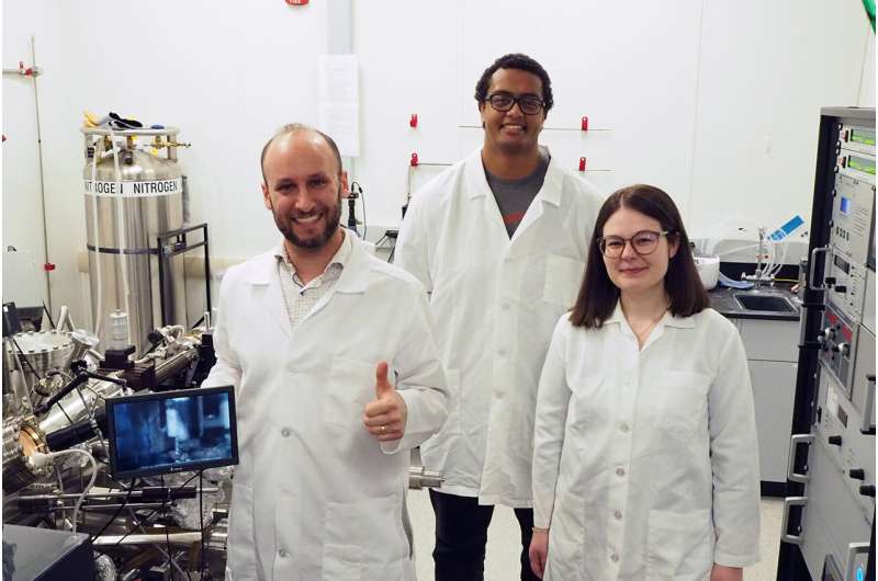
Tyler Cocker (left), Jerry Cowen Chair in Experimental Physics at Michigan State University, with doctoral students Stefanie Adams and Mohamed Hassan in the Ultrafast Terahertz Nanoscopy Lab. Credit: Matt Davenport/MSU College of Natural Science
These pulses consist of light waves at terahertz frequencies, meaning they oscillate up and down a trillion times per second. Recently, theorists showed that this is the same frequency at which defects in silicon atoms should oscillate back and forth inside a sample of gallium arsenide.
By coupling STM and terahertz light, the MSU team created a probe with unparalleled sensitivity for defects.
When the STM tip hit a silicon defect on the surface of gallium arsenide, a sudden, intense signal appeared in the team’s measurement data. When the researchers moved the tip one atom away from the defect, the signal disappeared.
“This was a flaw that people had been looking for for over forty years, and we could see it ringing like a bell,” Cocker said.
“At first it was hard to believe because it was so unusual,” he continued. “We had to measure it from every angle to make sure it was real.”
Once convinced that the signal was real, it was easy to explain thanks to the years of theoretical work devoted to the subject.
“When you discover something like this, it’s really useful when there are already decades of theoretical research that characterize it in depth,” said Jelic, who, along with Cocker, is also corresponding author of the new paper.
Although Cocker’s lab is at the forefront of this field, groups around the world are currently combining STM and terahertz light. There are also a variety of other materials that could benefit from this technique for applications beyond defect detection.
Now that his team has shared its approach with the community, Cocker is eager to see what other discoveries await.
More information:
Terahertz time-domain spectroscopy at the atomic scale, Photonics of nature (2024). DOI: 10.1038/s41566-024-01467-2
Provided by Michigan State University
Quote: Physicists develop method to detect single-atom defects in semiconductors (2024, July 4) retrieved July 4, 2024 from https://phys.org/news/2024-07-physicists-method-atom-defects-semiconductors.html
This document is subject to copyright. Apart from any fair dealing for the purpose of private study or research, no part may be reproduced without written permission. The content is provided for informational purposes only.